Lith Corporation, founded in 1998 by a group of material science doctor from Tsinghua University, has now become the leading manufacturer of battery lab&production equipment. Lith Corporation have production factories in shenzhen and xiamen of China.This allows for the possibility of providing high quality and low-cost precision machines for lab&production equipment,including: roller press, film coater,mixer, high-temperature furnace, glove box,and complete set of equipment for research of rechargeable battery materials. Simple to operate, low cost and commitment to our customers is our priority.
Thin Film Deposition System: Advanced Equipment for Precision Coatings
Overview
A Thin Film Deposition System is a sophisticated piece of equipment designed to deposit uniform, high-quality thin films onto a variety of substrates. These systems are essential in research, development, and industrial manufacturing, where precise control over film thickness, composition, and uniformity is critical. Thin film deposition systems utilize various technologies, including physical vapor deposition (PVD), chemical vapor deposition (CVD), thermal evaporation, sputtering, and atomic layer deposition (ALD), to create metallic, ceramic, organic, or hybrid coatings.
These systems are widely employed in industries such as electronics, optics, nanotechnology, energy, and materials science. By operating in controlled environments—typically under vacuum or inert gas conditions—they minimize contamination, ensure consistent deposition, and enable the fabrication of complex multilayer structures. Laboratory-scale, benchtop, and industrial-scale thin film deposition systems provide flexibility for experimentation, prototyping, and production.
Features
Modern thin film deposition systems are designed with several advanced features to ensure precision, reliability, and versatility:
1. High-Vacuum or Controlled Atmosphere Chamber
Stainless steel chambers can achieve ultra-high vacuum conditions or maintain a controlled gas environment to minimize contamination and optimize deposition quality.
2. Multiple Deposition Techniques
Systems may integrate thermal evaporation, sputtering, PVD, CVD, or ALD sources, enabling deposition of metals, oxides, nitrides, and complex multilayer structures.
3. Substrate Holders with Motion Control
Substrate holders can rotate, tilt, or oscillate to ensure uniform film thickness and coverage on flat and complex 3D surfaces.
4. Thickness and Rate Monitoring
Quartz crystal microbalance (QCM) sensors, optical monitors, or other in-situ measurement devices provide real-time feedback on film growth and thickness.
5. Digital Control and Automation
Programmable interfaces allow precise control of deposition parameters such as power, substrate temperature, gas flow, deposition rate, and process duration for reproducible results.
6. Safety and Maintenance Features
Vacuum interlocks, temperature protection systems, modular components, and automated purge cycles ensure safe operation and facilitate maintenance.
Process
The thin film deposition process depends on the selected technique but typically follows these general steps:
1. Substrate Preparation
Substrates are cleaned and pretreated to remove contaminants and enhance film adhesion.
2. Chamber Evacuation or Gas Control
The system chamber is sealed and evacuated or filled with a controlled atmosphere, creating optimal conditions for deposition.
3. Material Deposition
* Physical Vapor Deposition (PVD): Material is vaporized thermally or by sputtering and condenses onto the substrate.
* Chemical Vapor Deposition (CVD): Reactive gases form a thin film via surface chemical reactions.
* Atomic Layer Deposition (ALD): Alternating, self-limiting precursor pulses create conformal, atomic-scale films.
4. Monitoring and Adjustment
Deposition rate, thickness, and uniformity are continuously monitored, and parameters are adjusted as needed to maintain precise film properties.
5. Completion and Substrate Removal
After achieving the desired thickness, the system cools, the chamber is vented, and substrates are removed for further use or analysis.
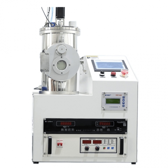
PVD Deposition System
Applications
Thin film deposition systems have extensive applications in both research and industrial settings:
* Electronics and Semiconductors: Fabrication of conductive, dielectric, and protective layers for integrated circuits, sensors, and MEMS devices.
* Optics and Photonics: Production of mirrors, anti-reflective coatings, optical filters, and multilayer optical devices.
* Nanotechnology and Materials Science: Creation of nanoscale thin films to study electrical, magnetic, and optical properties.
* Energy Devices: Coating of photovoltaic cells, batteries, fuel cells, and transparent conductive layers.
* Biomedical and Surface Engineering: Deposition of functional, biocompatible, or protective coatings on implants and medical devices.
Advantages
Thin film deposition systems offer several significant benefits:
1. High Purity and Quality: Controlled deposition ensures minimal contamination and excellent adhesion.
2. Precise Thickness Control: Real-time monitoring allows for accurate, reproducible film thickness.
3. Versatility: Supports deposition of a wide range of materials, including metals, ceramics, organics, and multilayers.
4. Uniform Coatings: Substrate motion and optimized chamber design enable consistent coverage even on complex geometries.
5. Scalability: Systems range from benchtop laboratory models to full-scale industrial equipment, accommodating various research and production needs.
6. Process Flexibility: Digital automation and programmable recipes allow customization of deposition conditions for specific applications.
Conclusion
The Thin Film Deposition System is a versatile and essential tool for producing high-quality coatings with precise control over material properties. Its combination of advanced deposition technologies, controlled environments, substrate motion, and real-time monitoring ensures reliable, uniform, and reproducible thin films.
With applications spanning electronics, optics, nanotechnology, energy devices, and biomedical engineering, thin film deposition systems play a critical role in modern research and manufacturing. Their ability to produce high-purity, uniform coatings on complex substrates makes them indispensable for advancing materials science, device fabrication, and surface engineering technologies.


 +86 13174506016
 Louis@lithmachine.com
 +86 18559646958
 18659217588
 English ▼


